Xanadu and GlobalFoundries plan 300 mm photonic quantum manufacturing
Source report: 2026-10-06 · Editorial analysis published: 2026-10-06
The October 6 partnership targets silicon nitride photonics and single-photon detectors at GlobalFoundries’ Malta, New York line. It announces a manufacturing pathway, rather than verified production volumes.
Analysis and practical implications
This section is our analysis and illustrative calculations, separate from the source report.
A manufacturing partnership for photonic hardware
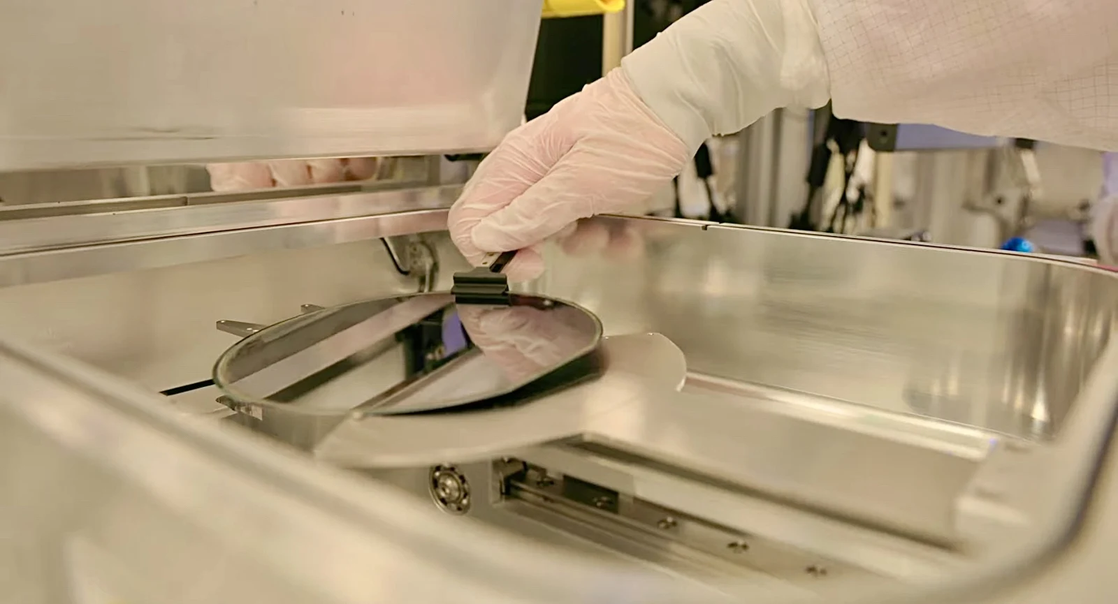
Xanadu announced a multiyear partnership with GlobalFoundries on October 6, 2026. The initial focus is industrializing ultra-low-loss silicon nitride photonics and superconducting nanowire single-photon detectors through the manufacturer’s 300 mm production line in Malta, New York. The collaboration aims to transfer existing Xanadu technology from laboratory prototypes toward industrial production. Its output is expected to support future fault-tolerant demonstrators and the longer-term objective of quantum data centres. The release does not provide completed production volumes or a customer delivery schedule.
This is relevant to computing infrastructure because a laboratory device and a repeatable manufacturing process solve different problems. A component may demonstrate useful behavior without being ready for reliable production in large numbers. Our interpretation is that the announcement addresses that transition. It should be tracked through manufacturing and system milestones, rather than reported as a completed quantum data centre. The proposed pathway is an industrial development effort whose operating results and commercial availability still need evidence.
What the two component types do
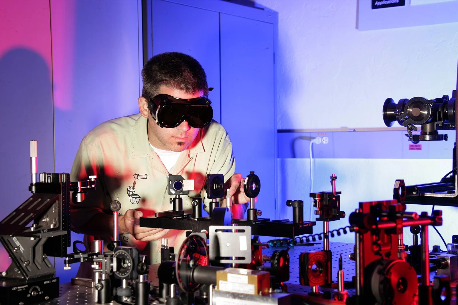
In the announced architecture, silicon nitride photonics guides light through optical circuits. The detector platform is used for photon-number-resolving measurement, which determines how many photons are in a pulse when reading calculation outputs. Xanadu expects the combination to improve system speed and reduce chip overheads, but does not publish a numerical benchmark for those expected benefits in this release. We retain the difference between the stated role of a component and an independently measured result from the combined system.
For a hardware comparison, the reader should identify which function each component performs and which metric describes that function. Optical loss, detector behavior and full-system computation are not the same quantity. An improvement in one may require changes elsewhere before it becomes a useful system-level improvement. This is our assessment framework for the partnership, not a finding about production parts already delivered. It is especially important when a release brings several technologies together under a broad claim about future computing scale.
A 300 mm wafer is not a 300 nm process node
The 300 mm figure is the diameter of the wafer used by the manufacturing line. It does not identify a 300 nm transistor process or provide a direct comparison with a mining ASIC’s fabrication node. Wafer format and the process used to create features on it describe different aspects of manufacturing. Our interpretation is that readers should retain that distinction when comparing announcements across photonics, electronics and specialized computing hardware. A shared semiconductor vocabulary does not make all of their performance measures interchangeable.
A larger production format can be part of a manufacturing strategy, but the headline diameter alone does not reveal the number of good components available per wafer. That depends on the design, process and production results. It also does not establish the cost of a finished module or the consumption of a working system. A useful manufacturing update would include the relevant qualification and yield evidence. We do not calculate a unit cost, a production capacity or an energy advantage from the 300 mm figure in this announcement.
Process transfer needs repeatability
Moving a design into a manufacturing environment requires more than reproducing one successful laboratory sample. The process must operate within tolerances that support the intended component behavior. A production review would examine variability, defect patterns, test methods and the criteria used to accept a device. These are general manufacturing considerations, not disclosed results for this partnership. The release establishes the plan to industrialize the technology without publishing a production qualification report or a measured distribution of component performance.
For infrastructure readers, repeatability is useful because a system depends on many parts behaving as intended over time. A high-performing sample may not describe an entire manufacturing batch. Test coverage and acceptance criteria help distinguish a demonstration from a reliable source of components. The next meaningful evidence would connect the transferred process with documented outputs and their suitability for integration. That would allow a reader to evaluate progress beyond the fact that an experienced foundry and a technology developer have agreed to work together.
Packaging and integration remain part of the system
A fabricated optical component still needs the interfaces that connect it with the rest of a computing system. Alignment, packaging, electrical control, testing and serviceability can all matter to the final device. Our analysis treats these as part of the implementation path rather than assuming the wafer line alone delivers a complete quantum computer. The announced manufacturing foundation is relevant, but it should not be confused with every engineering step required to make a commercial computing installation available to customers.
The same comparison discipline is familiar in ASIC mining. A chip does not become a working miner until the boards, power delivery, cooling, firmware and physical assembly meet the product’s requirements. The specific technologies differ, yet the distinction between a component and a usable system remains helpful. An infrastructure buyer should evaluate the complete delivered service and its operating conditions. The partnership does not disclose a mining product, a hashrate rating or a model-specific firmware package, and we have not added one on the basis of this news.
Quantum progress does not establish a Bitcoin mining shortcut
The release is about manufacturing photonic components and future quantum systems. It does not report an attack on Bitcoin, a demonstrated shortcut to SHA-256 proof of work or a commercial machine able to replace a mining fleet. Our interpretation is that a manufacturing milestone should remain attached to the task it actually addresses. Extending it to a claim about cryptocurrency security would require a separate technical result with a specified computation, resource estimate and reproducible evidence. Those results are not part of this announcement.
Likewise, there is no basis here for converting a quantum hardware development into an ASIC profitability estimate. Mining devices are compared using a defined algorithm, hashrate, electrical consumption and operating assumptions. The partnership does not provide an equivalent set of mining measurements. Readers can follow both fields without forcing unlike metrics into the same ranking. A meaningful connection to a cryptocurrency workload would have to demonstrate the relevant operation under stated conditions, rather than rely on the general phrase quantum computing.
Evaluate future demonstrations against their stated task
A future demonstration should identify the workload, the result expected from it and the conditions under which it runs. A hardware program can progress through component tests, integrated prototypes and larger systems, with each stage answering a different question. Our assessment is that these stages should remain visible in subsequent coverage. The manufacturing foundation may help the development program, but the announcement does not supply a benchmark that would allow an independent comparison of application performance or the economics of a production data centre.
A useful report would also distinguish planned capability from a result obtained on the system being described. Configuration, test duration, failures and the resources needed to repeat the experiment affect how a result should be interpreted. Comparing only a favorable headline metric can hide a system constraint or an unfinished dependency. Those considerations do not dismiss the partnership; they identify the evidence that will make it more informative. Clear measurement boundaries are as valuable for an emerging computing architecture as they are for a mature server or miner.
The milestones to watch after the agreement
The next developments to monitor are the transfer of the component processes, their qualification on the manufacturing line and integration into the planned demonstrators. Production quantities and the performance of accepted components would help connect the industrial program with the longer-term system objective. Commercial availability would need its own confirmation. This is our reading of the implementation path, not an undisclosed timetable from either company. The October 6 release does not set a verified ramp date, finished-system price or operating-site capacity.
For ASIC.tools readers, the news illustrates how specialized hardware reaches scale through a wider manufacturing and integration ecosystem. The practical takeaway is to compare announcements using the milestone actually achieved: a partnership, a qualified process, delivered components or an operating system. These are different forms of progress. Keeping them distinct makes it possible to follow photonic computing without treating a manufacturing plan as a finished installation or suggesting that a new technology has already changed the economics and security of present-day Bitcoin mining.
Source: Xanadu / GlobalFoundries ↗
Mining calculator ↗